CS641 class 22
More on Verilog
handout on
iverilog netlists
Always statement in Verilog
Always statement: uses procedural code, like initial, but does it over and over, not just once.
Left-hand side much be a reg
(recall rule for assign: lhs must be type wire)
reg A;
always @ (B or C)
A = B & C;
works like assign A = B & C
i.e., another way
to specify combinational circuitry
The execution of a procedural statement is triggered by:
· A value change on a wire
· The occurrence of a named event
always @ (B or C) begin // controlled by
any value change in B or C
X = B & C;
end
always @(posedge Clk) Y <=
B&C; // controlled by positive edge of Clk
always @(negedge Clk) Z <=
B&C; // controlled by negative edge of Clk
We can use “always” to model the snapshot behavior of D FF’s and
registers
What is the behavior of a D-flipflop ?
During every positive clock edge, the input is transferred to the output
See pg. C-53:
module DFF(clock,D,Q,Qbar);
input clock, D;
output reg Q; // Q is a reg since it is assigned in an always block
output Qbar;
assign Qbar = ~ Q; // Qbar is always just the inverse of Q
always @(posedge clock) // perform
actions whenever the clock rises
Q = D;
endmodule
Also see the Berkeley 61c handout for another version of DFF, with a RESET.
No testbed here, but we could modify the one for the RSFF.
This is a case where the reg turns into a real register in the resulting circuit. It is needed because the Qint reg can hold values that, because of the assigns to Q and Qbar, can be observed after the time they are set. Actually, it’s the first time we’ve seen a reg inside a module.
Finding out what components are used in the circuit: do “synthesis”, gen the netlist—see handout.
For synthesis, need to use iverilog on sf06, version .8x: later versions have lost synthesis capability!
FPGA: field programmable gate array: circuits be “programmed” i.e. built, by a machine from a program.
Verilog—>synthesis--> FPGA---> working circuit
Note we can add a reg to a module without causing a real register:
sf06.cs.umb.edu$
more mynandreg.v
// nand gate with “extra” reg that
doesn’t
// cause a
register in the circuit
module mynand(in0, in1,
out);
input in0, in1;
output out;
reg t;
assign out = t;
always @(in0 or in1)
t = ~(in0 &
in1);
endmodule
This has the same gates as mynand in its netlist.
Also the design using AND and NOT gates.
Here iverilog is smart enough to see that t is just passing its value through to out, so a register isn’t needed in the circuit.
With verilog, we can design with gates or Boolean expressions, and get working circuits out.
A Register in Verilog
Back to W’s 61c tutorial, look at pg.13, reg4
// positive edge-triggered,
// synchrounous
active-high reset.
module reg4 (CLK,Q,D,RST);
input [3:0] D;
input CLK, RST;
output [3:0] Q;
reg [3:0] Q;
always @ (posedge CLK)
if (RST) #1 Q = 0; else #1 Q = D;
endmodule // reg4
This reg will turn into a register, like the one in the DFF, to hold the sampled Q value for output.
We could write a TB for this like our old RSFF, setting signals manually at each point in time:
...
reg4 myreg(.CLK(CLK), .Q(q), .D(d), .RST(rst));
initial
begin
#0 rst = 1’b1; CLK =0;
#5 CLK =1; // expect new q = 0 at time +1
#5 CLK =0; rst =0; d=4’b0101; // changing rst and d while clk=0
#5 CLK =1;
#5 CLK =0; rst =0; d=4’b0111; // changing rst and d while clk=0
#5 CLK =1;
...
But this is boring, and get too many lines with monitor if it includes clk.
Using a Clock
signal in Verilog, with its own code separate from
the rest of the code
See idea on pg. 13, 15: get a clock going in the testbed module
reg4 myreg(.CLK(CLK), .Q(q), .D(d), .RST(rst));
initial
begin
CLK=1’b0;
forever
#5
CLK = ˜CLK;
end
initial
begin
#0
rst = 1’b1; // changing rst
and d while clk=0
#10
rst =0; d=4’b0101; // changing rst and
d while clk=0
#20
d=4’b0111; //...
$stop
The Accumulator
Circuit
pg 14: The accumulator circuit we discussed a while ago, now done in Verilog
Uses reg4 and also add4: we’ll get back to adders soon. Of course we could just write it as an expression
assign sum = x + y;
and let Verilog figure out something.
State Machines
parity checker: input 1001, output 0, input 10011, output 1, etc: even or odd number of 1s.
parityChecker: Note bug, need “xor #1 (...)”
Idea of buffer gate, needed here for Verilog. OUT = IN
Could use reg instead of DFF:
reg state;
always (@posedge CLK)
state = RST?0:IN^state;
assign out = state;
This will turn into a register/FF in the circuit
instead of ?, can use if/else or case. See pg. C-25 for case ( <= ensures parallel assigns, but not necessary here I think)
case statements are like C switches that don’t need breaks because they don’t fall from one case to another.
Nice testbed on pg. 17, showing how separate clock simplifies the test code. We only need to say what to do at 0, 10, 20,..., knowing that the clock will rise at 5, 15, 25, ..., well away from any delays in the system.
Note how we have to drive the system into each state and then out from there. Can be tricky. Can start over from initial state as needed.
This is simpler but similar to the early example of a finite machine to recognize 3 1s in a row.
Finite State Machine Example from Sequential Circuits
Handout: 3 ones…
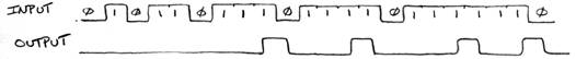
To do this, the system must be able to count ones up to 3, then start over. But it only needs memory for counts up to 2, because it can handle the last instance “on the fly”. So it only needs 3 states, S0, S1, S2 for how many ones already seen, and if in state S2 and sees another 1, report output=1.
Note fix from handout! S2 --> S0 on input = 1.
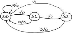
Need reg state to hold 0, 1, 2
Need to treat two ways out of each of three states--
Can set up case (state) inside always (@posedge clk), then in one case, tread input = 0 and input = 1 subcases.
Like reset of parityChecker, it would be good to have an init capability to force the system to state 0.
ThreeOnesChecker(OUT, IN, CLK, RST): same ports as parityChecker
Testbed: start with RST, then check self-loop, then 1 to go to S1, then 0 to go back to S0, then 1 to S1 again, then 1 to S2, then 0 to S0, then 1, and 1 again to get back to S2, then 1 to S0 seeing 1 output.
Adders
OK, thinking back, we had worked on building an adder

![]()
Clearly w can now build a 1-bit adder
module add1bit(a, b, c, s, c)
The challenge comes in wiring up 4 of these to make add4. Cover next time