Adders
Thinking back, we had worked on building an adder

![]()
Clearly w can now build a 1-bit adder
module add1bit(a, b, c, s, c)
The challenge comes in wiring up 4 of these to make add4. Cover next time
sf06.cs.umb.edu$
more add1bit.v
module
add1bit (a, b, c, s, cout);
input a,b,c;
output s, cout;
assign s = a^b^c;
assign cout = a&b|a&c|b&c;
endmodule
// add1bit
For a 4-bit adder:
module
add4 (a, b, s, ovf);
input [3:0] a;
input [3:0] b;
output [3:0] s;
output ovf;
wire [4:0] c;
assign ovf = c[4] ^ c[3];
add1bit bit0(a[0], b[0], 1’b0, s[0], c[1]);
add1bit
bit1(a[1], b[1], c[1], s[1], c[2]);
add1bit
bit2(a[2], b[2], c[2], s[2], c[3]);
add1bit
bit3(a[3], b[3], c[3], s[3], c[4]);
endmodule
// add4
module
add4_tb;
reg[3:0] a = 2;
reg [3:0] b = 3;
wire [3:0] s;
add4 myadder(a, b, s, ovf);
initial begin
#0 ;
#5 b = 2;
#10 a = 4; b = 4;
#15 a = -4; b = -4;
#20 a = -4; b = -5;
end
initial
$monitor("a = %b, b=%b, s=%b, ovf =
%b", a, b, s, ovf);
endmodule
// add1bit
sf06.cs.umb.edu$
vvp a.out
a
= 0010, b=0011, s=0101, ovf = 0
a
= 0010, b=0010, s=0100, ovf = 0
a
= 0100, b=0100, s=1000, ovf = 1
a
= 1100, b=1100, s=1000, ovf = 0
a
= 1100, b=1011, s=0111, ovf = 1
The
adder was a partial solution of our simple ALU:
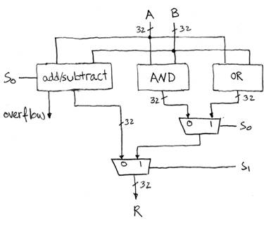
We see that this plan asks for a single unit to do add and subtract—is that doable?
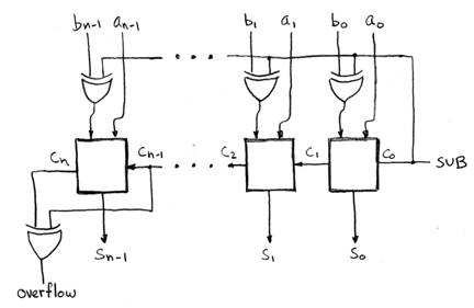
Subtraction is just addition by the additive inverse:
A – B = A + (-B)
and –B is obtainable by the rule ~B + 1. ~B is pretty easy to do. So we need an inverter slipped into the input side when doing SUBTRACT,
i.e. the needed input, B1 = SUB?~B:B
SUB B B1
0 0 0
0 1 1
1 0 1
1 1 0
Clearly B1 = SUB XOR B. So an XOR can be thought of as a conditional inverter.
To get the +1, we simply set carry-in to 1 for SUB, i.e. co = SUB.
Adder/Subtracter
Clearly we can modify add4 to addsub4 with an additional SUB input.
The AND and OR circuits are straight-forward.
So we could build this Simple ALU in Verilog
However, this is not a high-performance ALU, as discussed on pg. C-35. It needs to sequentially compute the bits, so for 32bits, it takes too long. See Section C.6, Faster Addition, if interested.
Another CPU Part: Register Files, on hw7
Pg. C-57: Verilog code
module
registerfile (Read1, Read2, WriteReg, WriteData, RegWrite, Datat1, Data2,
clock);
input [5:0]
Read1, Read2, WriteReg; // register
numbers, 0-31
input [31:0]
WriteData; // data coming in
input RegWrite, clock; // write enable, clock
output [31:0]
Data1, Data2; // output ports for reading two registers at once
reg[31:0] rf
[31:0]; // 32 registers each 32 bits
long
assign Data1 =
RF[Read1];
assign Data2 =
RF[Read2];
always begin
@(posedge clock)
if (RegWrite)
RF[WriteReg] <= WriteData; // write new data in RF
end
endmodule
See reg[31:0] rf [31:0]; // 32 registers each 32 bits long <--The internal memory, real registers in circuit
The register reading is not “clocked”. When you ask to read register 6, you get your wires connected to that internal reg (register).
The register writing is clocked. To write register 6, put the value on the wires connected to WriteData so as to be stable at the next clock edge, and make WriteReg = 6 and WriteData = 1. Then your value will be sampled at the clock edge.
Hopefully we now have covered enough of digital circuits for our needs.
We might need to come back to a few topics like hi-Z value.
Start Chap. 4 on the CPU
Note that the chapter is written so that readers can understand it without covering circuit theory, or very little about it. So there is some coverage that should be easy to read through. Try to read to Sec. 4.5 for next week.
The CPU
° Processor (CPU): the active part of the computer, which does all the work (data manipulation and decision-making)
• Datapath: portion of the processor which contains hardware necessary to perform all operations required by the computer (the muscle)
• Control: portion of the processor (also in hardware) which tells the datapath what needs to be done (the brain)
See Figure 4.2 for the
basic setup, where the datapath elements are in black and the control circuitry
in blue.